This ‘Made in India’ system would support research and development in nanotechnology
Bengaluru,, 18th December, 2017: Hind High Vacuum Co. Pvt. Ltd. (HHV), a vacuum science and technology company with major clients like HAL, ISRO, BARC, Titan etc, announced the launch of its first indigenously developed Atomic Layer Deposition (ALD) System based on technology transferred from IIT Bombay. This tool was developed entirely by HHV’s Thin Film Technology Division out of its Bengaluru facility as a part of the company’s on-going ‘Make in India’ initiative.
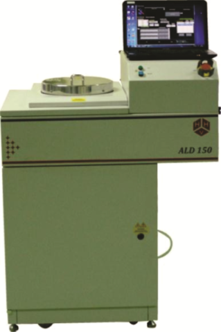
The ALD System would be initially supplied by HHV to academic and industrial institutions in India and abroad for research and development in the area of Nanotechnology. . The ALD process has gained interests in the fields of microelectronics and nanotechnology for manufacturing Nano films. Extensive research activity is on to improve the rate of depositions. The process improvements will make it commercially viable to find applications in various areas such as electronics, optics, energy, life sciences, sensors, instrumentation, medical, biological, mechanical, chemical, flexible devices, etc
“Atomic Layer Deposition (ALD) is a process technique that builds up thin film layers one monolayer at a time. The deposition technique gives great control over the thickness uniformity on three dimensional surfaces. Pin-hole free films can be deposited over large areas with extreme conformality, repeatability and precision. ” said Prasanth Sakhamuri, Managing Director of HHV. “ Researchers are currently developing ways to deposit metals and di-electrics in specific locations. The selectivity is the most important property for integration at 5 to 3 nanometer technology nodes. Looking ahead it is expected that ALD will play an increasingly important role in advancing semiconductor manufacturing and other applications.”
“Market analysis shows that the ALD technology is going to witness a compound annual growth rate (CAGR) of 19.1% from 2016-2021, leading to a global market size of almost $3.7 billion in the end year. HHV is now fully geared up to support the Indian and international research and businesses with its product offerings.” added Prasanth Sakhamuri.
For over 5 decades, HHV has been designing, developing and manufacturing off-the-shelf and customized deposition system products to fulfil the needs of scientific and industrial community. Its R&D team has been closely associating with world renowned scientists in thin film technology to develop challenging and advanced thin film deposition system products in this field. These unique thin film deposition equipments have been successfully demonstrated for functional performance, product quality and repeatability.
HHV is ranked among the global leaders in thin film technology with an international market spread. The group is particularly strong and competitive in executing large, and highly sophisticated customized thin film deposition equipment.
About HHV
Established in 1965 at Bangalore as a specialized enterprise to develop Indian self-reliance in high vacuum technology, HHV today serves a spectrum of Industries and R&D centers covering aerospace, atomic energy, defence, automotive, semi-conductors, electrical, horology, scientific instrumentation, decorative, food processing to name a few. HHV has an advanced research and manufacturing program in thin film technology, material science, metallurgy, astronomy, and special purpose machinery.
HHV works in three separate divisions based on specific technology:
- Vacuum systems & special projects
- Thin film equipment & contract manufacturing
- Optics & thin film coatings
HHV’s corporate office & manufacturing center is located at a 5 acre campus in Peenya industrial area of Bengaluru and its second manufacturing center in a 6.5 acre campus at Dabaspet, about 40 km’s from Bengaluru.
For more detailed information on HHV please visit: www.hhv.in